← pcb layout guidelines pdf Pcb routing guidelines for ddr4 memory devices pcb layout design guidelines [view 30+] schematic diagram to pcb layout converter →
If you are looking for Rf Pcb Design Guidelines Pdf - Encare you've came to the right place. We have 30 Pics about Rf Pcb Design Guidelines Pdf - Encare like PCI Express: PCIe PCB Manufacturing, Assembly, Design | MADPCB, PC & PCI cards - Engineering Technical - PCBway and also PCIe Layout and Routing Guidelines | Blog | Altium Designer. Here it is:
Rf Pcb Design Guidelines Pdf - Encare
PCIe Layout And Routing Guidelines | Blog | Altium Designer
pcie routing altium vias breakout pcb
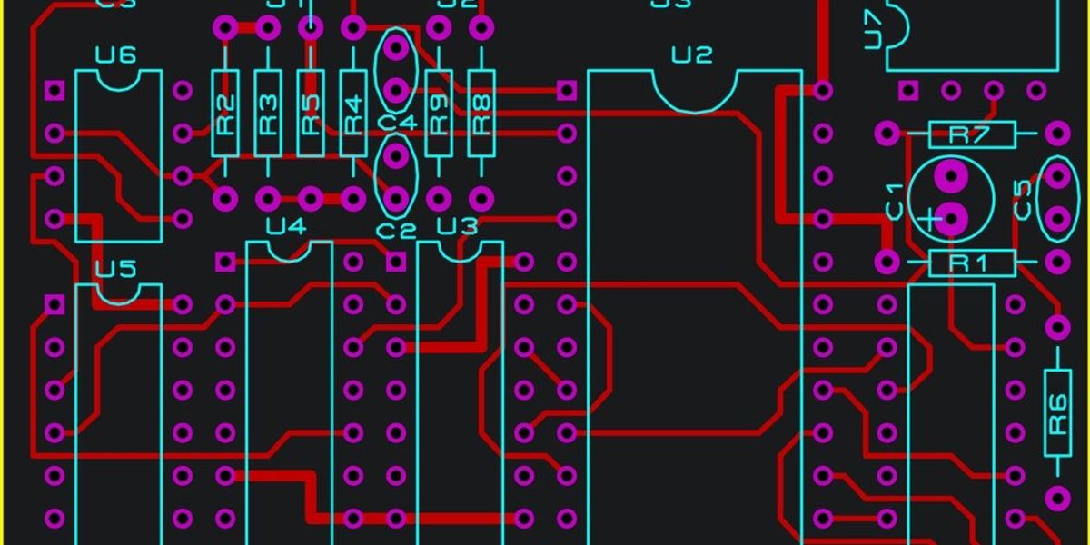
PCB Layout Guidelines.pdf
PCB Layout Guidelines.pdf
PCB设计软 件|印刷电路板|雷竞技技网页版Autodesk - 雷电竞Raybe
PCI Express: PCIe PCB Manufacturing, Assembly, Design | MADPCB
AN11082 PCB Design And Layout Guidelines For · PDF FilePCB Design And
PCIe Gen4 Standards Margin-Assisted Outer-Layer Equalization For Cross
pcie gen4 equalization margin lane outer cross transmitter link optimization frequency receiver keywords loop
TIDA-00423 用于 PCIe Gen-3 卡的高速前端参考设计 | 德州仪器 TI.com.cn
Make Sure To Consider These Factors When Creating A PCB Layout - Blog
pcb layout
(PDF) AN11082 PCB Design And Layout Guidelines For · PDF FilePCB Design
PC & PCI Cards - Engineering Technical - PCBway
pci card pcb pc circuit cards fingers bevelling pcbway board gold spacing contour boards multi
PCB Layout Guidelines.pdf
PCIe Layout Guidelines - YouTube
What Is PCIe (PCI Express)? | Sierra Circuits
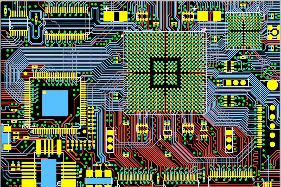
PCB Layout: A Comprehensive Guide
 www.wevolver.com
PCIe Layout And Routing Guidelines | Blog | Altium Designer
pcie routing altium
PCB Design Steps & Complete Guide | Cirexx
PCB Layout Guidelines.pdf
PCIe Routing Guidelines & Best Practices - Free Online PCB CAD Library
Diseño De PCB | Placa De Circuito | Solid Edge
PCIe Layout And Routing Guidelines | Blog | Altium Designer
pcie layout altium routing coupling
Pcb Layout Guidelines For Design - Vrogue.co
PCI Express Mini Card PCB And Connection Design - Parts Help - Fritzing
Your Guide To Flexible PCB Design & Layout
对华断供EDA软件!传美国将实施新的出口限制措施 Ssd新闻 存储新闻 - 闪德资讯
 www.0101ssd.com
Overview Of The PCIe 6.0 Standard | Zach Peterson | PCB Routing
PCB Layout Design For PCIe
PCB Layout Guidelines.pdf
A Detailed Guide To PCB Layout Design - IBE Electronics
Pcie gen4 equalization margin lane outer cross transmitter link optimization frequency receiver keywords loop. A detailed guide to pcb layout design. Pcie routing altium